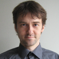
Assoc. Prof. Dr. Miroslav KOLÍBAL

Brno University of Technology, Czech Republic, EU
Position: Senior Researcher at the Institute of Physical Engineering, Faculty of Mechanical Engineering/ and CEITEC - Central European Institute of Technology/Brno University of Technology, Czech Republic
Specialization: Material science at micro- and nanoscale; 1D nanostructures; Modification and analysis of semiconductor surfaces; Electron beam induced processes
At the NANOCON´18 conference Miroslav Kolibal will present an invited lecture at the session A “Growth of quasi-1D semiconductors and oxides for nanoelectronics and nanophotonics in an electron microscope”.
Personal Background and Education:
- He carried out Ph.D. studies on applied physics at Brno University of Technology (Czech Republic) under supervision of Prof. Jiří Spousta developing Low Energy Ion Scattering (LEIS) in collaboration with Prof. Peter Bauer group (JKU Linz), defended in 2009.
- Later in 2009 he has joined the group of Dr. Milos Toth at FEI R&D in Hillsboro, Oregon (USA). After returning to Brno he has started an independent research in the field of nanowire growth and developed unique instrumentation and methodology for observation of nanowire growth in real-time in a scanning electron microscope.
- Being interested in one-dimensional nanostructures, he took the opportunity to join the group of Dr. Heike Riel at IBM Zurich Research Laboratory (Switzerland) in 2012, developing high-k dielectric templates for directed III-V nanowire growth. After return, he has joined a newly established centre of excellence CEITEC in Brno, Czech Republic.
Research Interests and main results:
- Growth of 1D semiconductor nanostructures with engineered properties targeting mostly nanophotonics (plasmonics) and plasmon-enhanced electrochemistry. This includes study of doping mechanisms, which lead to non-equlibrium dopant concentrations (above solubility limit) allowing e.g. to reach plasmon resonance in near-IR spectral range.
- Modification of surfaces and nanomaterials by electron/ion beams, which includes changes of surface termination, sputtering, growth, etching, oxidation, defect formation etc., thus allowing new strategies for nanoscale materials growth, manipulation and assembly.
- Development of instrumentation/methodology for real-time SEM observation of nanoscale processes in materials, e.g. growth, phase/structure changes etc. with emphasis on 1D semiconductors (nanowires and nanotubes). This research is done in close collaboration with ThermoFisher Scientific (formerly FEI) R&D in Brno.
Publication activity:
29 publications, 157 citations (without-self-citations)
More details: http://surfaces.fme.vutbr.cz/research/surfaces-and-interfaces/nanobb/
Back